


|
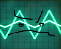
catbread.jpg posted:It's a boost converter, the low side switching is irrelevant to the classification, and indeed the only way to sensibly implement it, unless you're a masochist or only have access to p-channel devices. I say it operates more like a buck converter because when the switch is off the supply doesn't provide power, while in a boost supply the current is always flowing from the source. Therefore this circuit has the same power governing equations as a buck converter.
|
 #
?
Mar 2, 2009 07:59
#
?
Mar 2, 2009 07:59
|
|


|

|
| # ? May 21, 2024 18:47 |
|
|
Hey guys, I posted a while back about finding a traffic light and wanting to convert it into a set of musically triggered lights. The plan was to have the brightness of the lights modulated by the intensity of a musical input in certain frequency ranges, with red corresponding to treble, yellow to mids, and green to bass frequencies. I trawled the internet and finally found this circuit: http://wolfstone.halloweenhost.com/ColorOrgans/clofix_OptocouplerAmp.gif which I then converted to this-  Click here for the full 1201x654 image. I wanted to use the optoisolator design for safety etc, but apparently optoisolators require a pretty strong signal to work, so the op-amp section of the circuit is for voltage amplification. After that the signal is split into three, filtered to the desired frequency ranges and passed through the optoisolator. The voltage of this signal then goes into the gate of the triac which controls the brightness of the lamp. I've just got a couple of questions now- 1) Is there anything glaringly wrong with that circuit? I tried simulating it on LTSpice but I couldnt find the triac parts I was looking for so that was fruitless. 2)If you compare the images, you'll see that the original circuit runs from 120V AC, and my adapted one runs from 240V since I'm in the UK. Does anyone know which component values I'd have to change for this to work over here? 3)Could i replace the Line out input with a microphone input? Any help is much appreciated, thanks! Auspex fucked around with this message at 19:10 on Mar 4, 2009 |
|
#
?
Mar 4, 2009 18:54
|
|
|
I recently bought a ConnectOne Mini Socket iWifi and have been interfacing it with the Arduino. I'd like to be able to do a simple pass through from the serial monitor to the Mini Socket, but am having trouble making it work consistently. Anyone have ideas on how to drive two serial devices? Should I just buy a separate serial chip, or mux the iWifi Tx/Rx?
|
|
#
?
Mar 4, 2009 20:23
|
|

|
I recently had to reattach a couple caps I busted off my ipod when I opened it to fix the home button. What size are these things? They look smaller than even a 201 package, but I'm used to 603s so maybe I'm wrong about that. Excuse the file name, I originally thought they were ferrite beads. 
|
|
#
?
Mar 4, 2009 20:46
|
|

|
Hillridge posted:I recently had to reattach a couple caps I busted off my ipod when I opened it to fix the home button. What size are these things? They look smaller than even a 201 package, but I'm used to 603s so maybe I'm wrong about that. Excuse the file name, I originally thought they were ferrite beads. Well 0201 is the smallest I've come across, and they look like grains of sand. According to wikipedia, there's one size smaller, 01005, so I suppose it could be that... These small parts are a pain in the rear end if you have to do any rework. And they make PCBs harder to build  . I blame cell phone manufactures. . I blame cell phone manufactures.
|
|
#
?
Mar 4, 2009 21:42
|
|
|
well there I go. Soldering again. A friend on freenode told me I needed to buy this: http://www.seeedstudio.com/depot/digital-storage-oscilloscope-with-panels-p-167.html It's a aurdino based 1mhz Digital Ociliscope. It arrived in the mail two days ago.  I looked at what's in the package, and i'm kinda intimidated. There's a whole heck of a lot of SMT parts. And some very very small components. I need an o-scope. I couldn't resist. As a warmup, I ordered this capacitor meter kit. http://www.seeedstudio.com/depot/capacitance-meter-kit-p-268.html And tonight, after working a 12 hour shift, I sat down and soldered it. The best part is, it works. It took me roughly 90 minutes. I'm quite happy I managed to complete it first try. Here's the result of that labor:  Assembled using this:  I haven't really done a whole lot of soldering since my friend and I were doing the paintball gun boards. So heres' the kit I got. http://www.seeedstudio.com/depot/digital-storage-oscilloscope-diy-kit-65288with-panels-p-166.html I'm just so excited that it worked. And gave a valid result when I tested it against the stockpile of components I've built up. Speaking of components, a different friend got a bag of crap from www.woot.com at christmas. In the box, was a crapton of electronics. I just started sorting the bits and peices. There's lots of 1/2 watt resistors. A few large diodes. Maybe two transistors. a $3 relay. And I'm still sorting the rest.  This all does eventually tie into my spring project. Which is a voltage doubler and regulator for 6v electrical systems. What do you guys know of charge pumps? Alternatively i'm going to go with a small 2:1 transformer to get the voltage high enough for a SMPS or even linear regs to handle it. Nerobro fucked around with this message at 10:16 on Mar 5, 2009 |
|
#
?
Mar 5, 2009 09:53
|
|

|
That looks like a pretty awesome kit, I may have to pick one up to try it out. From the photos it looks like they put the hardest part on for you. I can't tell for sure, but it looks like a BGA, which would have been nearly impossible to do by hand. For the rest of the surface mount you'll just need some good tweezers, plenty of flux (I prefer liquid), and some patience.
|
|
#
?
Mar 5, 2009 14:21
|
|
|
Hillridge posted:I recently had to reattach a couple caps I busted off my ipod when I opened it to fix the home button. What size are these things? They look smaller than even a 201 package, but I'm used to 603s so maybe I'm wrong about that. Excuse the file name, I originally thought they were ferrite beads.
|
|
#
?
Mar 5, 2009 16:09
|
|
|
Auspex posted:Hey guys, Here's a circuit for the falstad circuit simulator. Just go here, and in the window that pops up go to file > import, then copy this into the window: code:As for making it compatible with 240V, you'll likely just need to double the gate drive resistors R4, R8, and R11. Also you'll want to make sure your triacs are rated for that much voltage.
|
|
#
?
Mar 5, 2009 16:51
|
|
|
That oscope looks sweet, I want one of those kits. I can't tell what size those components are though, wish they had a bigger picture. If you want to solder SMDs, buy a good pair of tweezers. You CANNOT effectively solder SMD without them, or at least w/out going crazy. Best trick I've learned is to put a crappy joint down on one side of the part to tack it down, put a good joint on the other side, then use some flux/extra solder to clean up the crappy joint. It's tedious, but I get good results. If it's 0805 parts or smaller, try to find a good magnifying glass, or retrofit a microscope. Good luck! What are you doing with charge pumps btw? I'm interested in learning some more about those...
|
|
#
?
Mar 5, 2009 23:48
|
|
|
I've only used charge pumps for a cheap way to create a negative voltage. I'm sure there are other good uses though.
|
|
#
?
Mar 6, 2009 00:56
|
|
|
Nerobro posted:well there I go. Soldering again. I've been bickering with a rep from Seeed on another forum for a while now. He's somehow convinced that their rates for PCB fabrication are lower than Gold Phoenix's, which is flat out wrong. They sell some interesting products, but it seems like all the Chinese companies out there refuse to accept that they might not offer precisely what you need. I will probably end up buying that o-scope kit, though. I tried my hand at surface mount soldering for the first time the other day:   I bought this kit: http://practicalcomponents.com/boards/solder-practice-pc003.htm which comes with dummy components to populate the board. The kit was about $15. If anyone is interested, I'd be willing to buy a bunch and resell them, since Practical Components isn't really set up to take individual orders very well (especially not over the internet.)
|
|
#
?
Mar 6, 2009 02:02
|
|
|
Very nice job. I see a few little blobs here and there, but nothing too messy. On that PLCC on the bottom, I think having more heat and/or using a slightly bigger iron tip may help. Otherwise, very good job!
|
|
#
?
Mar 6, 2009 04:13
|
|
|
clredwolf posted:Very nice job. I see a few little blobs here and there, but nothing too messy. On that PLCC on the bottom, I think having more heat and/or using a slightly bigger iron tip may help. The PLCC was the most retarded thing to solder. Looking at it under magnification, all the connections are electrically fine, and there are no solder bridges, but it's ugly. The rest was easy-peasy, though. I'll be soldering everything I can surface mount from now on.
|
|
#
?
Mar 6, 2009 05:09
|
|
|
clredwolf posted:That oscope looks sweet, I want one of those kits. I can't tell what size those components are though, wish they had a bigger picture. quote:If you want to solder SMDs, buy a good pair of tweezers. *SMT tips* quote:What are you doing with charge pumps btw? I'm interested in learning some more about those...
|
|
#
?
Mar 6, 2009 11:28
|
|
|
ANIME AKBAR posted:I say it operates more like a buck converter because when the switch is off the supply doesn't provide power, while in a boost supply the current is always flowing from the source. Therefore this circuit has the same power governing equations as a buck converter. If we want to get technical, it's a buck-boost converter because the inductor is alternately shorted to ground and connected to the load without drawing current from the supply. It also has the characteristic voltage ratio (of the buck-boost) of D/(1-D), which you can see by considering the integral inductor voltage. Very cool circuit nonetheless. It's using a form of current-mode control (as the output voltage is effectively fixed by the forward voltage drop of the LED). I'm currently designing a synchronous buck converter for a project, now that is a bitch. You have to play all kinds of tricks to control a high-side and low-side N-channel device with the same PWM signal without short-circuiting the supply, in this case a very crappy solar panel, with an output capacitor that I am very reluctant to short-circuit, not so much due to the SC current but the lost energy. Having both devices off at the same time creates the problem of where to put the inductor current, but that can be pretty easily solved with RC snubbers.
|
|
#
?
Mar 6, 2009 12:26
|
|
|
Has anyone ever used a 65.536 kHz (or faster) crystal as a secondary oscillator for a PIC? I would like full 16-bit accuracy for a real-time clock but the datasheet says explicitly that the secondary oscillator is supposed to be a watch crystal (32.768 kHz).
|
|
#
?
Mar 7, 2009 03:41
|
|

|
Because it goes with that little buck-boost supply. Here's the joule theif http://www.emanator.demon.co.uk/bigclive/joule.htm
|
|
#
?
Mar 7, 2009 04:33
|
|
|
BattleMaster posted:Has anyone ever used a 65.536 kHz (or faster) crystal as a secondary oscillator for a PIC? I would like full 16-bit accuracy for a real-time clock but the datasheet says explicitly that the secondary oscillator is supposed to be a watch crystal (32.768 kHz). I don't see why a faster one wouldn't work. Perhaps it has the load capacitors inside and they are sized for operation at that frequency? I'd just try it and find out. Can't really hurt. If you post the datasheet I might be able to see what's up. I'm assuming it just has a normal pierce oscillator. ANIME AKBAR fucked around with this message at 19:53 on Mar 7, 2009 |
|
#
?
Mar 7, 2009 19:31
|
|
|
catbread.jpg posted:It also has the characteristic voltage ratio (of the buck-boost) of D/(1-D), which you can see by considering the integral inductor voltage. I was interested in the circuit because I'm designing some simple LED drivers for another project. I wanted to drive a few sets of LEDs at good efficiency but without lots of circuitry. Couldn't find any ICs that could do the job without lots of complexity or cost, so I had to do it discretely. At first I drove each set of LEDs in a series string from a boost supply. The only feedback I had was measuring the supply voltage with an ADC and then having the MCU adjust the duty cycle to give the right power. But the calculations were a lot more complicated than I thought (takes several hundred instructions). With this one is a lot simpler (D and Vin are inversely proportional). And I can make my existing circuits into the new one just by connecting the cathodes of the LEDs to supply instead of ground. catbread.jpg posted:I'm currently designing a synchronous buck converter for a project, now that is a bitch. You have to play all kinds of tricks to control a high-side and low-side N-channel device with the same PWM signal without short-circuiting the supply, in this case a very crappy solar panel, with an output capacitor that I am very reluctant to short-circuit, not so much due to the SC current but the lost energy. Having both devices off at the same time creates the problem of where to put the inductor current, but that can be pretty easily solved with RC snubbers. One thing that always bugged me is that synchronous rectified supplies can't run in discontinuous mode (without some special protection). If the inductor fully discharges before the flyback switch opens, then current would start flowing from the output to ground through the inductor in the opposite direction. Then when it does opens... well it would suck. Are most supplies just not meant to operate in discontinuous mode, or do they all have some protection against this? I assume they must, since if they didn't simply detaching the load would destroy it. ANIME AKBAR fucked around with this message at 20:08 on Mar 7, 2009 |
|
#
?
Mar 7, 2009 19:46
|
|
|
ANIME AKBAR posted:I don't see why a faster one wouldn't work. Perhaps it has the load capacitors inside and they are sized for operation at that frequency? I'd just try it and find out. Can't really hurt. If you post the datasheet I might be able to see what's up. I'm assuming it just has a normal pierce oscillator. It doesn't have built-in load capacitors, so that wouldn't be it. I'd just try it out myself but I don't have one on hand at the moment. The datasheet has a diagram on page 142 of the oscillator internals and a description of the operation on page 143. It says that it is "a low-power oscillator rated for 32 kHz crystals" but I don't know enough about oscillators to know why it would or would not work with a faster crystal. Edit: Looks like a Pierce oscillator to me, though. BattleMaster fucked around with this message at 20:42 on Mar 7, 2009 |
|
#
?
Mar 7, 2009 20:37
|
|
|
ANIME AKBAR posted:Synchronous rectification design is pretty neat. One of the non consulting jobs I'd be fine having would be designing high end supplies for computers and instruments. Some of those things are absolutely ridiculous and have ripples in the tens of microvolts. I'm not sure how properly designed supplies deal with that. As long as my one can overcome the startup transient, the control is tracking the input voltage, and there's capacitors on the input and output, so I'm thinking the output capacitor can sink enough current until the load starts drawing enough to keep it continuous. Gonna start with a big-rear end inductor and then try and cut it down. It gets a bit tiresome here, as the time constant of the integral control is designed around the time constants of the switching, and of the output L-C network, so that will have to be adjusted as well.
|
|
#
?
Mar 7, 2009 22:12
|
|
|
Can somebody explain basic capacitors and how they work in a circuit? I know they store electrons and have a voltage. However, how do they work in a circuit? Do electrons ever pass THROUGH the capacitor? I was understand the impression that they NEVER pass through the capacitor (because of the insulator between the two dielectrics) However, this example circuit seems to contradict my thinking since it shows electrons flowing THROUGH the capacitor. Can soembody help me out? 
|
|
#
?
Mar 10, 2009 16:09
|
|

|
I'm contemplating getting into FPGAs for a battery-powered project, and with a few hours of searching it seems that the Actel IGLOO nano devkit at ~50 bucks is a pretty decent deal. It has the AGLN250 chip on it, for reference. Now, I'm curious as to how much power one could cram into this thing. Gates, Macrocells and VersaTiles means very little to me, so I was hoping for some general explanation (e.g. "you could build a USB stack in that!" or "yeah, the blinky LED demo patterns are about it"). Please help me out, and continue discussing FPGAs!
|
|
#
?
Mar 10, 2009 16:17
|
|
|
Snaily posted:I'm contemplating getting into FPGAs for a battery-powered project, and with a few hours of searching it seems that the Actel IGLOO nano devkit at ~50 bucks is a pretty decent deal. It has the AGLN250 chip on it, for reference. Now, I'm curious as to how much power one could cram into this thing. Gates, Macrocells and VersaTiles means very little to me, so I was hoping for some general explanation (e.g. "you could build a USB stack in that!" or "yeah, the blinky LED demo patterns are about it"). Honestly, I would recommend sticking with Xilinx/Altera. They are the two biggest FPGA manufactures and, while I haven't used Actel's tools, I've heard that most of the smaller vendors kinda suck as far as development environments go. You also might want to look into a larger CPLD, depending on what your design needs. They generally have lower power numbers than FPGAs and you don't have to worry about loading them at power on. As far as telling if your design will fit, it can be tough. The different FPGA vendors count things slightly differently, which complicates the problem even more. For example, I know Xilinx switched to a larger, 6 input LUT (look up table) starting at the Virtex 5, but then multiplied their datasheet numbers by a "correction factor" of 1.5 to match the traditional 4 input LUT. The downside of this "improvement" is that a good deal of existing designs were written to take advantage of a 4 input LUT-flip flop structure, and thus didn't see as much improvement by moving to the supposedly bigger device. Hmm maybe I should do a write up of basic FPGA tech... The best way to tell is to mock up a design and compile it. That way you know how full you will be before you start spending money. What are you planning on doing? I'm sure that would help people here make more informed suggestions...
|
|
#
?
Mar 10, 2009 16:39
|
|
|
SnoPuppy posted:Honestly, I would recommend sticking with Xilinx/Altera. They are the two biggest FPGA manufactures and, while I haven't used Actel's tools, I've heard that most of the smaller vendors kinda suck as far as development environments go. SnoPuppy posted:You also might want to look into a larger CPLD, depending on what your design needs. They generally have lower power numbers than FPGAs and you don't have to worry about loading them at power on. SnoPuppy posted:As far as telling if your design will fit, it can be tough. The different FPGA vendors count things slightly differently, which complicates the problem even more. SnoPuppy posted:Hmm maybe I should do a write up of basic FPGA tech... SnoPuppy posted:The best way to tell is to mock up a design and compile it. That way you know how full you will be before you start spending money. What are you planning on doing? I'm sure that would help people here make more informed suggestions...
|
|
#
?
Mar 10, 2009 16:52
|
|
|
Vinlaen posted:Can somebody explain basic capacitors and how they work in a circuit? The electrons don't go through. A yellow dot can never be found in the gap between the plates. The electrons go towards the first plate, and then stop. This builds up a field that pushes electrons away from the other plate.
|
|
#
?
Mar 10, 2009 16:56
|
|

|
Capacitors don't get interesting until you start using them in circuits with more than just DC voltages. To an AC signal, a capacitor behaves more like a resistor*. * - This is a generalization. Factors like frequency also play a part in this, and the phase of the current will differ from the phase of the voltage.
|
|
#
?
Mar 10, 2009 17:21
|
|
|
Snaily posted:I would, if I could find a comparable devkit compatible with a low-power chip. As a hobbyist, price tag does mean quite a lot, unfortunately. Digilent has what you need: http://digilentinc.com/Products/Catalog.cfm?NavTop=2&NavSub=400&Cat=Programmable%20Logic Their Dev boards have a lot of "extra" stuff that draw power in addition to what you'd be using, but if you were actually implementing a design, you wouldn't have to include that. Even at full tilt, they don't draw a boatload of power. The C-Mod might be what you're looking for (or a similar product), although I don't know if it has the capacity for what you'd like to do. The Data sheet for the XC2C64 says it draws less than 100uA at all times.
|
|
#
?
Mar 10, 2009 17:27
|
|
|
Hillridge posted:Capacitors don't get interesting until you start using them in circuits with more than just DC voltages. To an AC signal, a capacitor behaves more like a resistor*. It's exactly like a resistor! A resistor with a complex number for a value  Snaily posted:I would, if I could find a comparable devkit compatible with a low-power chip. As a hobbyist, price tag does mean quite a lot, unfortunately. Have you checked https://www.digilentinc.com ? They make a lot of Xilinx eval boards, and I'm sure that Altera has similar offerings. The development tools are free for those boards as well. Snaily posted:I was hoping for a SPI/SD card storage driver that could run at close to the maximum speeds allowed by the standard, with some data massaging beforehand. Maybe there's a better solution altogether? What is the other side of the interface? Just a simple data bus? Or something more complicated? A SPI core is fairly easy to implement and doesn't take up much space. Now, if you need to buffer data or compute checksums or other, more fancy operations, the design can become more complicated and require more resources. Edit: How fast do you want to run the SPI/SD interface? I know you said "close to the maximum speeds allowed by the standard", but that is still a bit vague. SPI doesn't have an official standard speed and SD cards have a number of standards - SD(high speed and low speed), SDHC, SDXC, maybe others I haven't heard of. SnoPuppy fucked around with this message at 18:03 on Mar 10, 2009 |
|
#
?
Mar 10, 2009 17:34
|
|
|
The Xilinx CMOD does look interesting, but perhaps too limited power-wise. I probably should dive into the development environments and see what happens and whether my ideas are workable at all.SnoPuppy posted:What is the other side of the interface? Just a simple data bus? Or something more complicated? Eventually, there'll be an imaging sensor, but until I figure the storage part out, I'm going to consider it as a 10-bit parallel signal. Presumably, there'd have to be some buffering, although I hope I can run it as a simple FIFO. SnoPuppy posted:Edit: I'm hoping for 50Mhz giving perhaps 25Mbit/s, although I'd really want to run it faster. I don't think the SD spec is possible to get at this point, though, so I'm stuck with SPI access.
|
|
#
?
Mar 10, 2009 18:33
|
|
|
Snaily posted:The Xilinx CMOD does look interesting, but perhaps too limited power-wise. I probably should dive into the development environments and see what happens and whether my ideas are workable at all. You should be able to run at your data rate - i.e. 50 Mbit = 50 MHz, 25 MBit = 25 MHz, etc. Depending on the FPGA, you could use DDR flops and then your clock only has to be half your data rate. Trying to compile the design will give you the best idea how much space it needs (obviously). I don't thinking about it more, I don't know if the CPLD would work because they tend to not have many flip-flops. But here's my estimate: A SPI interface can be implimented with a parallel-to-serial shift register and then all you would need is a small state machine and a shallow clock crossing FIFO. I imagine it could all be done with a few hundred flip flops and a handful of LUTs, with most of those being part of the FIFO. Granted, you probably want a bigger part if you plan on adding to it. And a bigger part can give you more breathing room in case you need to make a bug fix or something like that. Either way, the design will probably be very small. Also, remember that there isn't a strict SPI standard - it's more of a gentlemen's agreement. There is no standard on how many bits a transaction is, minimum setup/hold time, max clock frequency, etc. Make sure you read the datasheet of the device you're connecting to in order to figure all this out.
|
|
#
?
Mar 10, 2009 20:29
|
|
|
If any of you are interested in headphone amplifiers or Class D amplifiers I have just started a project over at HeadWize, one of the cool DIY headphone amplifier forums. I am hoping to have revision 1 of the design done by this weekend and hopefully get some prototype boards made by the end of next week. And for what it is worth the post I made was pretty informative on the Pros and Cons of class D amplification so IMO it is worth a read if you are interested in the technology behind amplifiers. http://headwize.com/ubb/showpage.php?fnum=3&tid=7767&fpage=9999 Now many of you who do know a thing or two about amplifiers will ask why are you going to make a design that powerful for headphones and the answer is simply because this is a technology that is incredibly underrepresented in the audio industry because there is a stigma that it sounds bad, when in reality a good design can sound better than the best Class AB amplifier on the market.
|
|
#
?
Mar 10, 2009 20:42
|
|


|
Vinlaen posted:Can somebody explain basic capacitors and how they work in a circuit? Individual electrons can't go through the capacitor (at least, not until the voltage across it is so high that the insulator breaks down, which usually destroys the capacitor). A current, however, can. What happens is that the circuit pushes an electron onto one plate, which repels an electron on the other plate and pushes it into the circuit on the other side. One electron goes in, one comes out. As more and more electrons get pushed on to the negative plate, and pushed off of the positive plate, the charge on those plates creates a voltage that pushes against the voltage in the circuit. When that voltage equals the external voltage being applied by the circuit, current will no longer flow through the capacitor. So in a setup like this: code:Things get more interesting when alternating current is brought in to the picture, because then, the capacitor usually doesn't have time to fully charge before the current changes direction and begins discharging it again. This means that it has a different effect on the circuit depending on the frequency of the AC. For a very high frequency, the capacitor barely has time to charge at all, and so acts almost like a direct connection, with very low impedance (impedance is like resistance, but a bit more complicated because of how it relates to the frequency and phase of AC). At low frequencies, it has time each cycle to charge up and oppose the current, and so it has a higher impedance.
|
|
#
?
Mar 10, 2009 20:57
|
|
|
SnoPuppy posted:You should be able to run at your data rate - i.e. 50 Mbit = 50 MHz, 25 MBit = 25 MHz, etc. Depending on the FPGA, you could use DDR flops and then your clock only has to be half your data rate. SnoPuppy posted:Trying to compile the design will give you the best idea how much space it needs (obviously). I don't thinking about it more, I don't know if the CPLD would work because they tend to not have many flip-flops.  GUI choices? GUI choices?SnoPuppy posted:But here's my estimate: That makes it sound like even the smallest proper FPGA dev system would work, but you're obviously right about the room to grow. I can't imagine the code I'd write to be very well tuned, either. SnoPuppy posted:Also, remember that there isn't a strict SPI standard - it's more of a gentlemen's agreement. There is no standard on how many bits a transaction is, minimum setup/hold time, max clock frequency, etc. Make sure you read the datasheet of the device you're connecting to in order to figure all this out.
|
|
#
?
Mar 10, 2009 21:31
|
|
|
It would be better if there was a strict standard, but at least SPI is so basic that it's usually easy to get your application working with any particular implementation of it.
|
|
#
?
Mar 10, 2009 22:20
|
|
|
Snaily posted:Assuming the SD card shuffles data away that fast, that's hopefully true. I personally like Xilinx because I already know their development tools, their architecture, their quirks and caveats, and have a good deal of experience with their FPGAs. None of this applies to you, however. Part of the reason I would suggest a major manufacture is that you are much more likely to find someone else who has used the tools and devices before. If you are using something more rare and need help, you might have a harder time finding someone who can tell you how to fix it. I also think that the Xilinx/Altera devices have more to offer than others, but it sounds like you wouldn't need those features for your design. Really, just try the toolchains and see which one is easiest to use/compile/simulate with.
|
|
#
?
Mar 11, 2009 00:02
|
|
|
Snaily posted:Now, I'm curious as to how much power one could cram into this thing. Gates, Macrocells and VersaTiles means very little to me, so I was hoping for some general explanation (e.g. "you could build a USB stack in that!" or "yeah, the blinky LED demo patterns are about it"). I'll take a crack at this. My work is a Xilinx shop, so I'm not too familiar with Altera/Actel/Lattice's various offerings. Here's what I know about FPGAs: ---------------------------GENERAL EXPLANATION OF FPGAS AND CPLDS---------------------------- Programmable Logic Devices come in two flavors: FPGAs and CPLDs. The basic idea behind both is that you write a description of what you want the chip to do (this is a little bit different than traditional proceamming), and then you use a special kind of compiler to turn your Verilog or VHDL code into a "binary". You then load the binary into your FPGA or CPLD and it works just like the chip was internally full of whatever logic gates and pin I/O you specified. The short difference between FPGA and CPLDs is: - CPLDs are non-volatile so all you need is the one CPLD. Flash your binary onto the CPLD and you're good to go. CPLDs hold much less functionality than FPGAs, so they're used for simple tasks usually. - FPGAs don't usually store their binaries, so you usually also need a PROM that loads the FPGA's binary on powerup. The smallest FPGAs are a lot more powerful than the largest CPLDs. You can use an FPGA for simple tasks or for complicated ones. ---------------------------SHE ASKED ME WHY I TOLD HER IT WAS "BIG"---------------------------- So how do we describe how 'big' an FPGA is? As others have pointed out, "equivalent gate count" is kind of an arbitrary rating, because FPGAs aren't internally made up of actual gates - they're made up of programmable 4-input lookup tables (4 input variables, 1 output variable). These are called LUT4s. A Xilinx "slice" has two LUT4s and two single-bit D flip-flops. FPGAs are made up of a bunch of slices, a wiring layer to connect slices together (you program this), and a bunch of extra poo poo (usually including blocks of RAM, digital clock managers/PLLs, and hardware multipliers). High-end FPGAs also often include an integrated microprocessor and an ethernet interfaces. So in 10 slices you could theoretically fit 20 bits worth of registers and probably enough glue logic to do whatever you want with those registers. The tricky thing about the "gate count" metric is that it's hard to account for things like BlockRAMs in your gate count. For example - the one of the FPGAs we're using at my work has sixteen 18kBit dual-port BlockRAMs embedded in it. If I had to implement that much RAM using gates, it could easily take 500,000 slices to implement. One 18kBit dual-port BRAM is big enough for a 16-bit FIFO that's 1024-levels deep. Many individual modules won't use more than one or two BRAMs. However, they don't share well - two different FIFOs will need two BRAMs even if the total amount of storage required is less than 18kBits. As a general rule of thumb, it's pretty hard to utilize more than 85% of an FPGA. The vendor tools will choke while trying to compile and optimize your design. Place-and-route (that's the term used for 'compiling') is much easier and gives better results at 70% than 85%, and below about 70% it's pretty easy to make everything fit. You can utilize almost all of a CPLD but it's still pretty tough to get 100% utilization. CPLDs are usually used for small, specific tasks. Usually a CPLD will be enough for anything which you could conceivably have built out of discrete chips, but will be too small for designs that have a lot of interfacing and flip-flops. FPGAs can do everything a CPLD does, but a gently caress ton more of it and also other tasks too. You can replace the "microcontroller and logic chips" paradigm with one single FPGA, even a fairly small FPGA at that. ------------- WHAT THE gently caress CAN I DO WITH THIS poo poo, POOPERNICKEL ----------------- Here are some of the devices that we use: small as poo poo: At my work, the very smallest programmable logic device we use is a Xilinx XC9536XL, which is a 36-macrocell CPLD. That chip is just barely large enough for a divide-by-10,000,000 clock divider, a divide-by-two clock divider, and some logic that switches the outgoing clocks (10MHz and 1 pulse-per-second) from being passthru to being internally generated if the external clocks get disconnected. We use 35 of the macrocells and I think 32 of the registers. small: The smallest FPGA we use is a Xilinx Spartan II-15k (XC2S15). Our design uses about 70% of the chip's resources and includes an 8-bit bus interface, 12 bytes of on-board storage (with interfacing), two large clock dividers (on the order of divide-by-1236), five smaller clock dividers (on the order of divide-by-50), a few 4-bit muxes, a limited I2C interface, and some internal mode control based on either jumper inputs or the bus interface. medium-small: The next up which we use is the Spartan II-50k. That one is at about 40% utilization and has everything listed above and also 4 extra bytes of storage, interfaces for two digital-analog converters and one analog-digital converter driver, and a much more complicated control system. medium: We're developing a board right now that uses the Spartan III-500k. That is a "large-size" FPGA with respect to simple tasks. That FPGA can easily hold more logic than you could ever hope to use up in a hobbyist design, in addition to two or three microcontrollers. You could probably cram in a soft-core microprocessor instead of a microcontroller, if you've got a copy of the Xilinx EDK. Once you get to the point where you start integrating a microprocessor into your FPGA, the limitation you typically hit is the amount of BRAM on the chip (since you need it for your instruction and data memory). If you're doing a microprocessor/microcontroller design, pick an FPGA with the right amount of BlockRAM and input/output pins and it's safe to assume that there will be plenty of logic slices for whatever you want them for. huge as poo poo: The largest chip we currently use is a Virtex-4 FX60. The "logic" portion of the design contains a 100-bit serial decoder for receiving timestamps, a state machine that converts decimal "time and date" into unix time, an 8-bit bus interface, 256 bytes of onboard storage, an 80-bit serial manchester decoder with CRC, a 16bit-by-512 FIFO, a 24-bit DAC driver, a high-fidelity PWM output (suitable for audio), and a few internal test waveform generators (triangle, sine wave). All of this uses maybe 20% of the chip's logic resources, 3 BRAMs, and 3 hardware multipliers. This design also uses the on-board PowerPC microprocessor with 64kB of instruction memory and 128kB of data memory, a UART interface, gigabit ethernet, and a ton of GPIO. Most of that stuff is provides as on-chip resouces, so it doesn't use up a ton of logic slices (maybe 5-10% of the chip). However, it uses approximately 100 BRAMs for everything. This is what drove our selection of such a large FPGA, the amount of BRAM. ------------- GIVE ME A TLDR, rear end in a top hat ----------------- TL;DR - In the Xilinx FPGA world (the only one I'm familiar with), I would call a 36 macrocell CPLD "pretty loving small", and a 256 macrocell CPLD would be "small but big enough for intelligent glue-logic." A 15k-gate Xilinx FPGA (although remember gate count is not a good metric) is "big enough for a lot of simple stuff", a 50k-gate FPGA is "big enough for some pretty sophisticated stuff", a 500k-gate FPGA is "big enough for a microprocessor to fit inside along with your logic", and big FPGAs like the Virtex-4VFX60 are "big enough to pretty much stuff a whole loving computer in there". Poopernickel fucked around with this message at 22:23 on Mar 11, 2009 |
|
#
?
Mar 11, 2009 10:36
|
|
|
Poopernickel posted:Algebraic! I'm going to assume that the small actors try to state comparative data to the Xilinx behemoth. Now I need to figure out VHDL/Verilog! It was touched upon before, but any hints or resources? I suppose I should go for VHDL as I'm Europe-based...
|
|
#
?
Mar 11, 2009 11:43
|
|

|

|
| # ? May 21, 2024 18:47 |
|
|
Snaily posted:Algebraic! I don't have a good 'gut feel' for what you guys use over there in Europe. In America, both VHDL and Verilog are very common. VHDL puts a lot of emphasis on type definitions, parameters, and spelling out e-v-e-r-y little detail of your design. This makes for clean, modular cores that you can take from design to design, but it's kind of a pain in the rear end. I think Verilog is easier to learn, faster to develop in, and more intuitive than VHDL. Especially if you know how to program in C, which Verilog was modeled after. At the risk of starting a serious nerd flame-war, I would push you to learn Verilog instead. Altera has excellent Verilog support and releases most of its own cores in Verilog. Xilinx's ISE tool suite (used for making strictly Verilog/VHDL/schematic-based designs) has really good Verilog support, but all of the cores provided in Xilinx's EDK (which is used for embedding microprocessors and code) are written in VHDL. You can still use Verilog cores alongside VHDL cores, but it's a little bit clumsy at times. Xilinx's tech support also seems to all be VHDL-trained instead of Verilog-trained. Now how to learn Verilog - that is the question indeed. I don't put a whole lot of emphasis on book learning when it comes to Verilog. I have a few books that I use as references, but you will never learn to program by reading about it. I would recommend buying a dev board with an FPGA and some headers/LEDs and poo poo already on it, and learning to make some simple designs. All of the FPGA houses give out free/lite versions of their software. In the case of Xilinx, the free version (called 'webpack') is actually pretty much full featured. It doesn't support the high-end FPGAs of each line, but who cares about that. Some good example designs would be passing a pushbutton input through to an LED or turning an LED on and off at a rate of 1Hz (divide this from whatever clock you have). Maybe also running the button input through a one or two second delay. Those are pretty much the "hello world" of FPGA programming. If you're used to working in the microcontroller world, the first thing you'll figure out is that FPGAs are a whole lot less limited than microcontrollers. There is a lot of stuff that's trivial in Verilog but a pain in the rear end on a microcontroller. Also you have a whole ton more I/O pins. A typical FPGA has between 100 and 500 I/O pins available to whatever the heck you want with. Drive strength varies from device to device, but most FPGAs can theoretically drive or sink 20mA of current. Probably not on every pin at the same time though. Another thing you will come to realize is that clock speeds are much slower in the FPGA world than they are in the microcontroller / microprocessor world. A "holy poo poo that's impressively fast" FPGA design might run at 400MHz. A "that's pretty fast" design might have a section or two running at 250MHz, a section or two running at 100MHz, and then a few sections running at slow clock speeds. A "fast enough for normal people who aren't crazy" design might run at between 10 and 25MHz. Poopernickel fucked around with this message at 22:23 on Mar 11, 2009 |
|
#
?
Mar 11, 2009 18:18
|
|