


|
clredwolf posted:It's a great little program actually, but it does no simulation and it does not automatically lay traces (which is half the reason to use a PCB making program). The free version of Eagle is a bit harder to use, but can automatically figure out the best way to connect everything together and lay traces for you. In my experience, 99.99% of the time where the Auto-router is used, you end up with a board that won't work properly (i.e. susceptible to EMI), as they're all variations on "Drunkard dragging a wet bit of string around". this page: http://www.alternatezone.com/electronics/pcbdesign.htm has a good tutorial including examples of what, and what not to do when laying out boards.
|
 #
¿
Jan 10, 2008 00:31
#
¿
Jan 10, 2008 00:31
|
|


|

|
| # ¿ May 2, 2024 09:56 |
|
|
I found that toner transfer using paper took too long, and was too much hassle as it took me 3 or 4 tries (at 15 minutes each go) before I got something that I could etch. Using Press-N-Peel blue available here, is much quicker, and nine times out of ten transfers perfectly on the first attempt. mrbill posted:I now have a Tek 453 scope on the way. I received a Tek TDS2012B scope yesterday  with a current probe on the way. with a current probe on the way.
|
|
#
¿
Jan 23, 2008 00:56
|
|

|
babyeatingpsychopath posted:I model this thing in LTSpice, and the waveform looks good. When I wire it on the breadboard, the LED is always on. What did I do wrong? If I don't hook the 555 to voltage, the LED is NOT on, so I know that's doing something. The most likely problem is that something is hooked up wrong. Double-check your wiring and component pinouts. It is also possible although less likely, that your transistor is leaky/damaged. Try another one.
|
|
#
¿
Feb 9, 2008 23:32
|
|
|
Nerobro posted:So, tonight I actually got some silicon hooked up on my bicycle headlight project. I'm using a 7805 vreg to cut down the power from a 9.6v 2.3ah battery pack. I'm looking to drive 50leds at 20ma each. That butts right up against the limit of the 7805. The 7805 is rated to max current of either 1A or 3A (depending on the version) and only with an adequate heatsink. If you need more current output (and you do), you can use a shunt circuit something like this: http://www.rason.org/Projects/vreg/vreg.htm R1 and R2 are used to increase the output voltage, so aren't necessary for your application. you should also have a 5.1V Zener connected between Vout, and Gnd, which will clamp the voltage to a non-LED destroying level if the 7805 fails.
|
|
#
¿
Apr 1, 2008 23:30
|
|
|
ante posted:What a classmate of mine started doing out of frustration at our limited options, was just using a cellphone charger. Just a quick word of warning, if the charger is 1) switchmode, and 2) has a two pin (ungrounded) plug, the output may float at half your mains voltage (wrt ground) due to one or more class Y1 capacitors which may be connected between the primary (mains) and secondary (5V) circuits to lessen EMI. see the schematic here on page 6 (CY1 is the capacitor in question). This can be more than enough to destroy sensitive parts... and damage some not so sensitive parts if you plug in connections to other grounded equipment while things are powered up. SMPSs with a 3 pin plug (i.e. they're grounded) or linear supplies don't have this problem.
|
|
#
¿
May 18, 2008 23:01
|
|
|
why not do two gain stages in series each with a gain of somewhere around 10? The LM324 is a quad opamp IC after all, and this will give you an overall gain of 100 leaving one opamp free for an output buffer. Other thoughts: is a gain of 100 close to your supply rails? Even though the LM324 can work on a single supply, you'll still need to bias your input signal. something like: 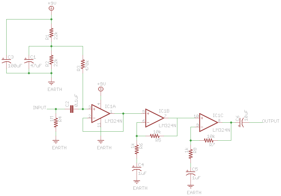 This should give a voltage gain of 121 (11x11). R1 and R2 set your bias voltage, in this case 4.5V or half of the supply (9V, but 12V should be fine) Because resistors (and active components) have thermal noise, and reactances (capacitors/inductors) don't, we add some more components to our biasing network... C1 (47uF, the value like everything else in the schematic, was just chosen arbitrarily) is used to decrease thermal noise from the biasing resistors by shunting it to ground, R3 is a high value resistor (any value higher than 470k is fine) to 1) stop the voltage divider being loaded down by whatever you're biasing, and 2) the lower current through the resistor = the lower the noise. Edit: your volume control should be after the output of the gain sections, otherwise you're just moving your input closer to the noise floor and amplifying that. Edit2: clarification? Noise a result of EMI/RFI is not what I'm talking about. Resistors: have Thermal noise proportional to their absolute temperature (in degrees Kelvin), current noise proportional to the current through them, and some more noise depending on what they're made from (carbon is noisier than metal film). Inductors generate as much noise as a piece of wire does, i.e. next to none, yes it's always there but for practical purposes it can be ignored. If your electrolytic capacitors aren't bubbling, you're doing it wrong. 
Chalupa Joe fucked around with this message at 21:20 on Jun 13, 2008 |
|
#
¿
Jun 13, 2008 09:39
|
|
|
Jonny 290 posted:
If you'd like to avoid possible electrocution, it is absolutely imperative that you do this. As for ground loops... in a linear supply, your primary and secondary sides should be electrically isolated? Chalupa Joe fucked around with this message at 10:54 on Jun 17, 2008 |
|
#
¿
Jun 17, 2008 10:52
|
|
|
Snaily posted:I'm fairly sure this is exactly what the mirror command in Eagle CAD does. It is: In the schematic editor MIRROR flips the symbol over so that your nets can be laid out clearly without messes of wire going everywhere. In board layout MIRROR moves a component (or group of components) from one side of the board to the other. Of course... in board layout view, you're looking down on the top (component side for through hole) of the board, anything on the bottom layer appears to be "backwards" but when the actual PCB is made, it ends up around the right way.
|
|
#
¿
Jun 26, 2009 22:16
|
|
|
I don't get what you're trying to do? maybe some pictures would help? is PINSWAP is what you need... From the Manual Cadsoft posted:Pinswap�and�Gateswap The PINSWAP command will swap the pins of non-polarised components (resistors/inductors/some capacitors), i.e. This is the same as physically putting the device in "backwards" Or for things like logic gates, will swap input pins since they are equivalent (you'd do this to make the board easier to lay out). GATESWAP is for things like dual op-amps etc. where you have multiple copies of the same thing in one package.
|
|
#
¿
Jun 27, 2009 01:32
|
|
|
dv6speed posted:I'm looking for a product, kind of like a heat sink grease, that can be applied to mechanical electrical connections to help improve electrical conductivity and prevent future oxidation of the metal. Switch lubricant, or Contact cleaner with lubricant is what you're looking for.
|
|
#
¿
Jul 24, 2009 04:40
|
|
|
ANIME AKBAR posted:I posed the same question on the altera forums, and got a snarky reply from an admin that any output ports defined in your top level file will be assigned to pins, whether or not they were done explicitly in the pin planner. I normally have a few ports in my design that are only there for the sake of simulation, and aren't pinned out manually, so they were being randomly assigned pins during compilation. I still have no idea why this is the case or how to prevent it, and was pretty much told to deal with it by the admin. Anyways, removing the extra ports in my design appeared to solve the issue, but it's a pain in the rear end to have to add and remove ports every time I want to simulate. I'm assuming by simulation you mean the waveform viewer? You can prevent this "problem" by not assigning ports (which get mapped to pins on the device either explicitly by you, or implicitly by the compiler) to internal signal nets, and instead, naming your internal nets something other than "wire000001" or whatever they default to. These internal signals can all be accessed from within the waveform viewer. When you add signals it defaults to a filter of "pins: all" but you can change it to show nets/registers/etc. It's not a problem in Quartus, there's a difference between what you're telling the software to do, and what you want the software to do. Edit: had some terminology mixed up. Chalupa Joe fucked around with this message at 04:43 on Apr 9, 2010 |
|
#
¿
Apr 9, 2010 04:30
|
|
|
AnomalousBoners posted:I talked to a well learned man about this today and he suggested getting an analog multimeter to test the caps. The reason being it allows you to see a quick spike and then the discharge... Though apparently we have cap testers here at school....so yea I will probably be bringing them in here. Also yes these are polarized "can type" caps. It's a good idea to have both an analogue and a digital multimeter as there are situations for both types where one gives nonsensical measurements where the other doesn't.
|
|
#
¿
Dec 14, 2010 10:32
|
|
|
Slanderer posted:Curved lines?! That's just weird Wires going through components? That's just wrong.
|
|
#
¿
Jun 5, 2011 21:57
|
|
|
Silver Alicorn posted:Here's an issue, though. The inverter board used some sort of RoHS solder, so I had to alloy it with my own to get it to melt, and it left some solder plugs in the vias. I tried a solder sucker and three brands of solder wick, and I couldn't get them clear, so I ended up just dremeling it out, which may or may not have damaged the vias. Is there something obvious I missed here? Yes, melt the solder, then poke a wooden toothpick into the hole, thus displacing the solder for easy wicking... Or, if you have spare hands, or some means of holding the board steady: heat one side of the hole, and use a solder sucker on the other side sucking the molten solder through the board, alternatively there's the much more dangerous version of this method: melt the solder and blow it out of the hole with compressed air (this is a terrible idea, please don't do this). 
Chalupa Joe fucked around with this message at 08:38 on May 2, 2012 |
|
#
¿
May 2, 2012 08:34
|
|
|
This is probably anecdotal, but all the ones I've replaced were 10V rated CapXon brand capacitors, in the range of 1000-3300uF. They don't appear to be low ESR, so standard caps are probably fine to use. Panasonic caps of the same value, 16 or 25V and minimum 85�C temp rating depending on space are what I've used for replacements
|
|
#
¿
Aug 6, 2012 22:04
|
|
|
Stabby McDamage posted:I'm using EAGLE to design a PCB with a big giant matrix of connections. I could whip up a spreadsheet of connections very easily, but hand connecting them in EAGLE would be tedious to the max. Is there a way to automate import of bulk connections? I'm not sure what you mean by matrix, but would using a BUS (a multi-wire net) instead of multiple single NETs help? It should be possible to script but it's not something I've ever looked into.
|
|
#
¿
Jan 19, 2015 04:17
|
|
|

|
| # ¿ May 2, 2024 09:56 |
|
|
Autodesk have released their updated version of Eagle after buying out CadSoft , and basically if you haven't switched to KiCad yet, now is a good time. Always on subscription only pricing is the main thing people are upset about, the standard licence is limited to 2 layers (it was 4), and routable area for the free version has been halved. Chalupa Joe fucked around with this message at 19:23 on Jan 23, 2017 |
|
#
¿
Jan 23, 2017 07:30
|
|